This year I got a chance to acquire one of the first DM&P Vortex86EX2 SoC based system (ICOP VEX2-6427-5C4NE specifically). Comparably to my article about DM&P VortexDX3 SoC, I assembled the short article with the information which I had gathered from sources like dmesg, /proc/cpuinfo (NetBSD, SparkyLinux), datasheets, official web sources and images.
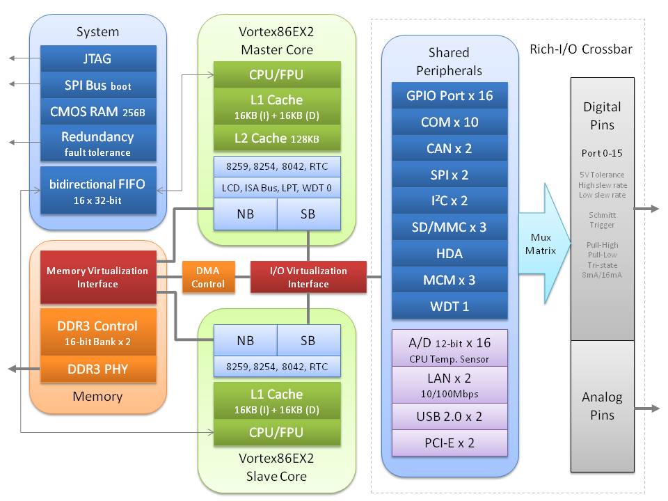
Below you can find the main Vortex86EX2 specifications (mainly taken from the official page, but supplemented by some information from BIOS and operating system messages, as well as hardware info):
- Identified as DM&P A9133 in BIOS.
- Master/slave design, two independent cores (as per my understanding, they cannot be used in the same Operating system at the same time).
- CPUID is 0x38504d44 (not sure yet if only the master one only or both).
- Frequency is up to 600MHz for the main core and 400MHz for the secondary one.
- 6-stage pipeline (both).
- 2x DMA controller (both).
- Integrated FPU (both).
- 16KB I-Cache, 16KB D-Cache (both), 4-way 128KB L2 Cache with write through or write back policy (main only).
- DDR3 control interface, up to 2GB RAM, 16-bit data bus, 2 ranks, clock support up to 400MHz, supports ECC.
- Real time clock (both).
- 65 nm manufacturing process.
- HD-Audio (Realtek ALC262 is used in my system).
- 2x USB 2.0 (ID: 6061) + USB device (PCI ID:1061).
- ISA bus interface (PCI ID: 6013):
- AT clock programmable.
- 8/16 Bit ISA device with Zero-Wait-State.
- Up to 3 SD/MMC cards (my board has one on the SoC module and one on the board). Supports SDSC, SDHC and SDXC. eMMC is also supported, up to version 5.1.
- 2x CANbus 2.0A/2.0B.
- 2x SPI controller.
- Up to 10x COM ports.
- 2x Fast Ethernet (10/100Mbps), my board has 1xR6040 model 6.
- 3x Motion Control Interface.
- Crossbar interface.
- 128 programmable I/O pins (GPIO).
- Temperature sensor.
- Package: 19x19mm, LFBGA-441.
- Operating temperature -40 to 85℃.
| Vortex86EX2 Specs and Block Diagram |


According to /proc/cpuinfo CPU supports CMPXCHG8B, CMOV, FXSAVE/FXSTOR instructions, MMX and SSE, SSE2 and SSSE3 extensions, even NX bit (using PAE?), thus seems to be the most advanced DM&P SoC in this regard. It also supports page size extension (4MB), physical address extension (PAE), SYSENTER/SYSEXIT instructions and time stamp counter. Because of above it can be likely classified as i686-compatible CPU (it loads i686 Linux kernel successfully). FPU is built-in on both cores. It does not have integrated GPU, thus external is needed (company is offering Vortex86VGA mini PCI-E card solution). My board has 4 USB 2.0 ports, but two of them provided by Genesys Logic's GL850G hub controller (USB ID: 0x0608). Additional information also can be found in CWID report in cpu-world.com (report has apparently incorrect halved cache sizes). /proc/cpuinfo can be found below.
/proc/cpuinfo (combined from NetBSD 9.99.69/Sparky Linux 4.19.0-6-686):
processor : 0
vendor_id : Vortex86 SoCcpu family : 6
model : 0
model name : Vortex86EX2
stepping : 2
cpu MHz : 600.032
cpu MHz : 600.032
physical id : 0
siblings : 1
core id : 0
siblings : 1
core id : 0
cpu cores : 1
apicid : 0
initial apicid : 0
fdiv_bug : no
f00f_bug : no
coma_bug : no
fpu : yes
fpu_exception : yes
cpuid level : 3
wp : yes
flags : fpu pse tsc msr pae cx8 apic sep pge cmov pat mmx fxsr sse sse2 nx cpuid pni ssse3
bogomips : 1200.06
clflush size : 32
cache_alignment : 32
address sizes : 36 bits physical, 32 bits virtual
power management:
 |
CPU-Z 1.94.0 screenshot (through wine, L2 is not detected properly) |
Note: There is no way to boot into slave CPU on my board, so all actual information is based on master one.
No comments:
Post a Comment